From: http://forums.parallax.com/forums/default.aspx?f=7&p=1&m=111286#m111354
 David
B says:
David
B says:
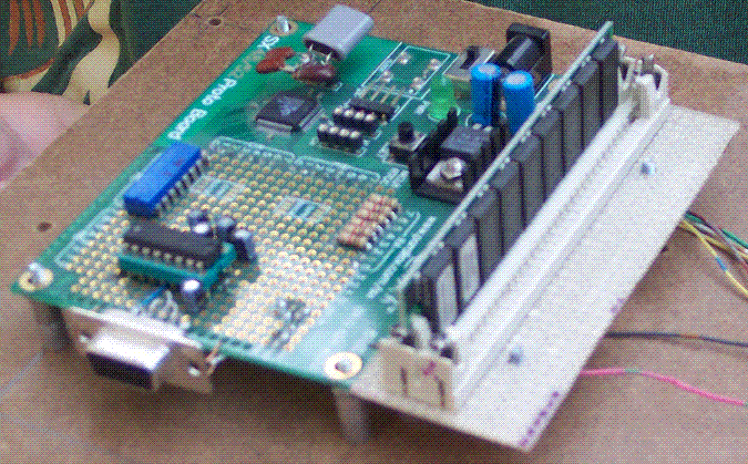
I used a SIMM and socket from an old motherboard I had in the garage, fastening the socket to an extension I attached to the side of the SX52 experiment board.This was mostly an educational experience, to learn about using dynamic RAMs, and to test whether DRAMs might be a worthwhile way to go in a logger, since I already have a few dozen SIMMs sitting around the garage.
It seemed to work just fine. The DRAM performed exactly as some document I'd found said they would, as soon as I found the magic number of delays to stick into various places. I haven't used it in any serious logger, but don't see any reason it wouldn't work just fine.
I'd been worried about satisfying the refresh requirements, but as I was using RTCC-controlled interrupts anyway for RS232 communication, I was able to just stick a refresh command into the ISR and it worked like a champ.
Here's some code. I was developing a bike speedometer/heartbeat sensor at the time, so you'll see lots of semi-developed code for those things. But the dynamic RAM and the RS232 ISR parts were working perfectly.
This demo uses a single 1 meg SIMM. It has routines to write to any individual address, read from any address, or to use it like a stack - write (push) to the next write address, or read (pop) from the next read address. And it does the DRAM refresh.
It includes RS232 send and get routines that let a PC communicate with the board. A few tests are built in - from a PC, you can send a character to the board to ask it to push a value to RAM, or send another character to pop from RAM and return the value to the PC. This way, you can push a few dozen characters, then pop them back to show the RAM is working. There also is RS232 code built in to run a Seetron LCD display. DRAM refresh is managed by the same ISR that runs the RS232 routines.
SIMM address lines are multiplexed into two parts, rows and column, of equal size. Since each address line is used twice, each additional line quadruples the capacity, rather than just doubling it. SIMMs come in 256K, 1, 4, and 16 meg sizes. 256K SIMMs have 9 pin row and column addressing, for 2^9 x 2^9 = 2^18 bytes, = 256K. So 256K needs 9 address pins, 1M use 10 pins, 4M use 11 pins and 16M use 12 pins. I used a 1 meg SIMM, but built the board to use all 12 address lines, so this design should be able to handle any of the sizes of DRAM.
The SIMM socket I used can hold two SIMMs. The column address strobe (CAS) is the chip select, so by using 16 meg SIMMs and two separate CAS lines, this same design should be able to control up to 32 megabytes of storage. But I haven't coded in the second CAS usage, or tried using 2 SIMMs. If 2 were used, the code would have to know when to switch over to the second CAS line, otherwise use of the higher addresses would just result in rolling over to point to address zero again. I measured that my SIMMs were 1 meg by testing for and detecting just this rollover.
When running from a 12V battery, at 20 mHz clock rate, the whole board draws 79 milliamps. Without the SIMM, it draws 74, so the SIMM itself seems to use about 5 mA at rest. I wasn't accessing the SIMM during this test, so I don't know if an active SIMM would be different.
I include a couple of documents that were helpful. But as I was learning how to do this, I also scanned the internet quite a bit and browsed many documents altogether to learn the general dynamic RAM process. But no single one of these other documents seemed comprehensive enough to include here.
My board includes a MAX232 to drive the RS232 to the PC. I used a 1K resistor array in the data bus to the RAM for protection in case I accidently set both the RAM and the SX data port to output at the same time. There are also resistors for protection of a few general purpose IO wires, one of which runs the Seetron LCD.
; sx52logger.src
; David Beals 2/25/2006
;
; operate a dynamic RAM
; Send characters to LCD (9600 baud)
; Receive and send characters over RS232 to run demo routines (9600 baud)
;
;-------------------------------------------------------
device SX52,OSCHS2
IRC_CAL IRC_FAST
freq 20_000_000
reset start_point
;-------------------------------------------------------
; variable assignments and name declarations
; Sx IO pin usage
PC_OUT equ ra.0 ; serial out to MAX232 to 9-pin 'D'
PC_IN equ ra.1 ; serial in to MAX232 to 9-pin 'D'
LCD_OUT equ ra.2 ; serial out directly to Seetron LCD
; ra.5-7 unused
; rb: unused
; RC: dynamic RAM data bus
; RD: dynamic RAM address low byte
; RE: lo nybble: RAM address hi nybble
; RE: hi nybble: DRAM control
;----------------------------------------------------------------
; Scenix model-based macros
SX48_52
bank52 macro 1
expand
bank \1
noexpand
IF \1 & %10000000
expand
setb fsr.7
noexpand
ELSE
expand
clrb fsr.7
noexpand
ENDIF
endm
mode52 macro 1
expand
mov w, #\1
mov m, w
noexpand
endm
;----------------------------------------------------------------
; Dynamic RAM macros
;
; Note: CAS_2 is connected to the DRAM2 socket.
; While untested, second SIMM socket should work, but would probably
; require code changes when transitioning from one SIMM to the other.
; Would need to add CAS_2 macros (to re.5) similar to CAS_1 below.
MEMORY_DELAY macro ; 20 mHz clock -> 50 ns per command.
nop ; 100 ns delays OK
nop
endm
DROP_CAS_1 macro
MEMORY_DELAY
clrb re.4
MEMORY_DELAY
endm
DROP_RAS macro
MEMORY_DELAY
clrb re.6
MEMORY_DELAY
endm
RAISE_RAS macro
setb re.6
endm
RAISE_CAS_1 macro
setb re.4
endm
RAISE_CAS_AND_RAS macro
setb re.4
setb re.6
endm
DROP_WE macro
MEMORY_DELAY
clrb re.7
MEMORY_DELAY
endm
RAISE_WE macro
setb re.7
endm
REFRESH macro
clrb re.4 ; drop CAS
MEMORY_DELAY
clrb re.6 ; drop RAS
MEMORY_DELAY
setb re.6 ; raise RAS
MEMORY_DELAY
setb re.4 ; raise CAS
endm
;-------------------------------------------------
FIFO macro
dw $047
endm
;-------------------------------------------------
; variables
org $A
flags ds 1 ; A
inbuffer ds 1 ; B
pointer1 ds 1 ; C
gtemp ds 1 ; D
; flag bits used by "flags" variable
FROM_PC_FLAG = 0
MEMORY_IN_USE = 1
FIFO_IN_USE = 2
org $10
bank_rs232 = $
txCount ds 1 ; 0
txDivide ds 1 ;
txLow ds 1 ;
txHigh ds 1 ;
rxCount ds 1 ;
rxDivide ds 1 ;
rxbyte ds 1 ;
rxHigh ds 1 ;
command ds 1 ;
rxStop ds 1 ; 9
org $20
bank_LCD = $
lcdtxCount ds 1 ; 0
lcdtxDivide ds 1 ;
lcdtxLow ds 1 ;
lcdtxHigh ds 1 ;
string ds 1 ;
fifoCount ds 1 ; 5
org $30
bank_ram = $
ramDatabyte ds 1 ; 0
popAddr1 ds 1 ;
popAddr2 ds 1 ;
popAddr3 ds 1 ;
pushAddr1 ds 1 ;
pushAddr2 ds 1 ;
pushAddr3 ds 1 ;
addr1 ds 1 ;
addr2 ds 1 ;
addr3 ds 1 ;
data ds 1 ;
readAddr1 ds 1 ;
readAddr2 ds 1 ;
readAddr3 ds 1 ; D
org $40
bank_assort = $
t1 ds 1 ; 0
t2 ds 1
t3 ds 1
t4 ds 1
t5 ds 1
hiNybble ds 1
loNybble ds 1 ; 6
letter ds 1
;-------------------------------------------------------
; interrupt service routine. Called on RTCC rollover.
;-------------------------------------------------------
;
; RTCC timing calculation/adjustments
;
; Four things combine together to determine rep rate of each ISR task:
; 1. crystal speed
; 2. ISR-exit adjustment to RTCC
; 3. RTCC divisor, if used
; 4. Counting down within each ISR task
;
; 9600 baud needs 1/9600 * 10^6 -> 104.167 usec between bits.
; 20 mHz crystal -> 20 cycles per usec
; 20 * 104.167 -> 2083 Scenix clock cycles between bits.
; Power of 2 that divides 2083 to a number between 0-255 -> 2083/16 = 130
; RTCC must count 130 -> 126 to 256 so reset RTCC upon exit to 126 (0x7E)
; So we need divide-bys totalling 16.
int_period equ $7E
ENABLE_INTERRUPTS macro ; 1001xxxx 1=RTCC->addr1 0=enabl int 0=cpu->rtcc 1=clk fall edge
mov !option, #%10010000 ; xxxx0000 = prescale -> RTCC; = divide clock by 2
endm
; hardware divide-by 2 means we need 16/2 = divide-by 8 in the task-skipping:
N_9600_FULL = 8
N_9600_1_5 = 12
N_STOPS = 8
;----------------------------------
org $0
ISR
; Transmit RS232 to LCD.
;
; Two ways to send:
; 1. User prepares txHigh, txLow, txCount. ISR sends until txCount is 0.
; 2. User fills 8-character FIFO then sets FIFO_IN_USE flag. ISR sends fifoCount bytes.
; Nothing to transmit if txCount is zero and the FIFO is empty.
bank52 bank_LCD
test lcdtxCount ; If bits to send, continue to send routine.
jnz :lcdxmit ; Otherwise check if the FIFO contains stuff.
jnb flags.FIFO_IN_USE, :lcd_end ; if FIFO empty then we're done.
FIFO ; pop next byte outa FIFO
mov lcdtxHigh, W ; and prepare it for sending.
mov lcdtxLow, #0 ; preset the start bit.
mov lcdtxCount, #11 ; prepare bitcounts: 10 = 1 stop bit, 11 = 2, etc.
djnz fifoCount, :lcdxmit ; After "fifoCount" bytes, the FIFO is empty.
clrb flags.FIFO_IN_USE ; so clear the flag.
:lcdxmit
djnz lcdtxDivide, :lcd_end ; skip "n" ISR occurrances.
mov lcdtxDivide, #N_9600_FULL ; Only xmit every nth pass.
dec lcdtxCount ; decrement bitcount
stc ; Create stop bit(s) to rotate onto tail of byte
rr lcdtxHigh ; LSB of data -> carry
rr lcdtxLow ; carry -> bit 7 of lo; start -> bit 6.
movb LCD_OUT, /txLow.6 ; apply bit to output port. (Invert if no MAX232)
:lcd_end
; Transmit RS232 to PC. Like above but no FIFO usage.
bank52 bank_rs232
test txCount ; If bits to send, continue in send routine.
jz :t_end ;
:xmit
djnz txDivide, :t_end ; skip "n" ISR occurrances.
mov txDivide, #N_9600_FULL ; Only xmit every nth pass.
dec txCount ; decrement bitcount
stc ; Create stop bit(s) to rotate onto tail of byte
rr txHigh ; LSB of data -> carry
rr txLow ; carry -> bit 7 of lo; start -> bit 6.
movb PC_OUT, txLow.6 ; apply bit to output port.
:t_end
; Receive a byte from PC.
; The received byte is available to the user when FROM_PC_FLAG is set.
test rxStop ; First check if waiting for stop bits to pass
jz :receive ; go on to normal processing when rxStop is zero
djnz rxStop, :r_end ; skip receive if we're still receiving stop bits
:receive
test rxCount ; If we're receiving byte
jnz :rxbit ; then go to bit-receive part;
movb C, PC_IN ; otherwise see if port holds startbit.
jc :r_end ; No startbit? done!
mov rxDivide, #N_9600_1_5 ; We see startbit. Set 1.5 delays,
mov rxCount, #8 ; and prepare to get 8 bits,
jmp :r_end ; and then wait for first data bit.
:rxbit
djnz rxDivide, :r_end ; Skip "n" ISR occurrances.
mov rxDivide, #N_9600_FULL ; Preset 1.0 delays next call.
movb C, PC_IN ; Read input pin into carry.
rr rxByte ; Roll carry into received byte.
djnz rxCount, :r_end ; If more bits to get, then skip stop bit part below.
setb flags.FROM_PC_FLAG ; All data in. Tell user that a byte is ready,
mov rxStop, #N_STOPS ; then prepare to skip n bits worth of passes
mov inbuffer, rxByte ;
:r_end
; refresh dynamic RAM every ISR call (13 microseconds) (if DRAM is not in use)
; 256K (2^18) has 512 (2^9) rows; 512 * 13 -> 6.6 milliseconds. should be ok.
jb flags.MEMORY_IN_USE,:m_end
REFRESH
:m_end
;----------------------------
; and finally, exit the ISR.
mov W, #int_period ; preset RTCC for correct timing of
retiw ; next interrupt for 9600 baud
;-------------------------------------------------------
; some strings
hello dw 'Hello World! HaWaYa?',0
itIsNow dw 'Feb 25, 2006 9:27 AM',0
;-------------------------------------------------------
; main program
;-------------------------------------------------------
start_point
call @init
call @splashScreen
; Spin until something needs attention:
:loop
jb flags.FROM_PC_FLAG, @:processPC
jmp @:loop
;----------------------------------------
; Jump based on incoming character.
;
; A: echo 'Y' back to PC
; B: read all dynamic RAM data and return to PC
; C: return 3 byte dynamic RAM current write address to PC
; D: push a letter to RAM
; E: pop next character from RAM and send to PC
; F: send splashScreen to LCD
:processPC
clrb flags.FROM_PC_FLAG ; Clear the "used" flag
cje inbuffer, #'A', @:commandA ;
cje inbuffer, #'B', @:commandB ;
cje inbuffer, #'C', @:commandC ;
cje inbuffer, #'D', @:commandD ;
cje inbuffer, #'E', @:commandE ;
cje inbuffer, #'F', @:commandF ;
jmp @:loop
:commandA
mov W, #'Y'
call @sendWtoPC
jmp @:loop
:commandB
call @sendAllToPC
jmp @:loop
:commandC
call @sendPushAddr
jmp @:loop
:commandD
call @pushLetter
jmp @:loop
:commandE
call @popnext
jmp @:loop
:commandF
call @splashScreen
jmp @:loop
;-----------------------------------------------------------------------------------
; end of main
;-----------------------------------------------------------------------------------
; demo: push character to RAM
_pushLetter
bank52 bank_assort
mov W, letter
call @pushRAM
bank52 bank_assort
inc letter
cjbe letter, #'z', :done
mov letter, #'A'
:done
retp
;-----------------------------------------------------------------------------------
; pop character from RAM and send to PC
_popNext
call @popRAM
call @sendWtoPC
retp
;-----------------------------------------------------------------------------------
; Scenix initialization
_init
mode52 $1F ; in/out direction mode (0 out 1 in)
mov !ra, #%11111010 ; a:
mov !rb, #%11111111 ; b:
mov !rc, #$FF ; c: in for now. Program will modify this.
mov !rd, #0 ; d out
mov !re, #0 ; e out
mode52 $1E ; pull-up resistor mode (0 enable 1 disable)
mov !ra, #%00000101 ; ins pulled-up
mov !rb, #0 ; ins pulled-up
mov !rc, #0 ; pull up all Cs
mov !rd, #$FF ; D out: DRAM address 0-7
mov !re, #$FF ; E out: DRAM address 8-11; controls
bank52 bank_rs232 ; RS232 init
clr txCount ; clear RS232 transmit flag
clr rxStop
bank52 bank_ram
clr pushAddr1
clr pushAddr2
clr pushAddr3
clr popAddr1
clr popAddr2
clr popAddr3
clr flags
bank52 bank_assort
mov letter, #'A'
setb rb.2 ; The SEETRON LCD requires about a second
call @delay1s ; to initialize. Keep its line set for that time.
ENABLE_INTERRUPTS
retp
;------------------------------------------------------------------
_splashScreen
call @lcdLine1
mov W, #hello
call @sendString
call @lcdLine2
mov W, #itIsNow
call @sendString
call @delay1s
call @clearScreen
call @delay1s
retp
;-------------------------------------------------------------------------------
; SendAll is not tested. Like, how would this react if zero bytes in DRAM?
;
_sendAllToPC
bank52 bank_ram
clr popAddr1 ; by clearing the pop address each time,
clr popAddr2 ; we may repeat the DRAM read if we want.
clr popAddr3
mov readAddr1, pushAddr1
mov readAddr2, pushAddr2
mov readAddr3, pushAddr3
:readMore
call @popRAM
call @sendWtoPC
bank52 bank_ram
cjne popAddr3, readAddr3, @:readMore
cjne popAddr2, readAddr2, @:readMore
cjne popAddr1, readAddr1, @:readMore
retp
;-------------------------------------------------------
_sendString
bank52 bank_LCD
mov string, W
:loop
mov W,string
mov M, #0
iread ; reads value from 11-bit code address in M, W
test W
jz @:end
call @sendWtoLCD
inc string
jmp @:loop
:end
retp
;------------------------------------------------------
; send character in W to PC via RS232.
; First wait for transmit buffer to be empty, then
; prepare transmit parameters, including the character
; and the number of stop bits.
; Setting txCount starts transmission.
_sendWtoPC
bank52 bank_rs232
:wait1
test txCount ; If bits being sent,
jnz @:wait1 ; wait
mov txHigh, W
mov txLow, #0
mov txCount, #10 ; 10 = 1 stop bit, 11 = 2, etc.
retp
;------------------------------------------------------
; Send character in W to LCD via RS232.
; Wait for hardware FIFO to become empty;
; Wait for transmit buffer to be empty.
; Then prepare transmit parameters, including the character
; and the number of stop bits.
; Setting lcdtxCount starts transmission.
_sendWtoLCD
bank52 bank_LCD
:wait1
jb flags.FIFO_IN_USE, @:wait1
:wait2
test lcdtxCount ; If bits being sent,
jnz @:wait2 ; wait
mov lcdtxHigh, W
mov lcdtxLow, #0
mov lcdtxCount, #10 ; 10 = 1 stop bit, 11 = 2, etc.
retp
;----------------------------------------------------------
; write the value 0-255 in W to LCD as two hex bytes.
_sendHexToPC
call @byteToHex
bank52 bank_assort
mov W, hiNybble
call @sendWtoPC
bank52 bank_assort
mov W, loNybble
call @sendWtoPC
retp
;----------------------------------------------------------
; write the value 0-255 in W to LCD as two hex bytes.
_sendHexToLCD
call @byteToHex
bank52 bank_assort
mov W, hiNybble
call @sendWtoLCD
bank52 bank_assort
mov W, loNybble
call @sendWtoLCD
retp
;--------------------------------------------------------------------
; convert binary byte in W to two ASCII Hex digits '0'-'F'
_byteToHex
bank52 bank_assort
mov loNybble, W
mov hiNybble, W
swap hiNybble
mov W, #$F
and loNybble, W
and hiNybble, W
mov W, #'0' ; Adding the char having the value "0" translates
add loNybble, W ; a numeric 0 to the ASCII "0".
add hiNybble, W
cjb loNybble, #':', @:s1 ; The colon ":" is one beyond "9" in ASCII,
add loNybble, #7 ; so if a ":" is seen then we need to skip
:s1 cjb hiNybble, #':', @:s2 ; 7 characters to get us to ASCII "A".
add hiNybble, #7
:s2 retp
;--------------------------------------------------------------------
_lcdline1
mov W, #$FE
call @sendWtoLCD
mov W, #$80
call @sendWtoLCD
retp
_lcdline2
mov W, #$FE
call @sendWtoLCD
mov W, #$C0
call @sendWtoLCD
retp
_clearScreen
mov W, #$FE
call @sendWtoLCD
mov W, #$01 ; clear screen
call @sendWtoLCD
retp
;-----------------------------------------------------------
; Jump table.
; You can JMP to any address, as long as the page is properly set.
; But can only CALL to the "lower" half of the eight 512 ($200) byte pages:
; SI: 000-0FF, 200-2FF, 400-4FF, 600-6FF, 800-8FF, A00-AFF, C00-CFF, E00-EFF
; NO: 100-1FF, 300-3FF, 500-5FF, 700-7FF, 900-9FF, B00-BFF, D00-DFF, F00-FFF
;
; This is located at 0x400, the start of an eligible code bank.
; Above here is code that doesn't change much, which may possibly
; extend into address 0x400 if enough changes are made.
org $400
init jmp @_init
delay1ms jmp @_delay1ms
delay10ms jmp @_delay10ms
delay100ms jmp @_delay100ms
delay1s jmp @_delay1s
delay10s jmp @_delay10s
sendString jmp @_sendString
sendWtoLCD jmp @_sendWtoLCD
byteToHex jmp @_byteToHex
sendHexToLCD jmp @_sendHexToLCD
sendHexToPC jmp @_sendHexToPC
pushRAM jmp @_pushRAM
popRAM jmp @_popRAM
clearRAM jmp @_clearRAM
sendPushAddr jmp @_sendPushAddr
sendPopAddr jmp @_sendPopAddr
readRAM jmp @_readRAM
writeRAM jmp @_writeRAM
lcdline1 jmp @_lcdline1
lcdline2 jmp @_lcdline2
clearScreen jmp @_clearScreen
clearSXRAM jmp @_clearSXRAM
sendWtoPC jmp @_sendWtoPC
sendAllToPC jmp @_sendAllToPC
pushLetter jmp @_pushLetter
popNext jmp @_popNext
splashScreen jmp @_splashScreen
;--------------------------------------------------------------------------
; clear Scenix RAM
_clearSXRAM
mov w,#$0a ;reset all ram starting at $0A
mov fsr,w
:zero_ram
clr ind ;clear using indirect addressing
incsz fsr ;repeat until done
jmp :zero_ram
retp
;----------------------------------------------------------
; Dynamic RAM configuration
;
; pushAddr1 is used for the low row addresses bit 0-7
; pushAddr2 is used for the low column addresses bit 0-7
; pushAddr3 bits are alternated between rows and columns for the high bits.
; 256K DRAM: bit 0 -> row bit 8; bit 1 -> column bit 8
; 1M DRAM: bit 0-> row 8, 1-> col 8, 2->row 9, 3->col 9
; 4M DRAM: same thing. Bits 0-5 used.
; 16M DRAM: same thing. All bits used.
;
; For 256K DRAMs, when push or pop Addr3 bit 2 becomes set then overflow has occurred.
; 1M: bit 4 is set on overflow
; 4M bit 6 set on overflow
; 16M: increment of Addr3 results in zero.
;
; Sure would be nice to automatically set this...
; Like, write number to addr 0.
; If addressing 256K+1 gets the number in 0 then this is a 256K device.
; If addressing 1M+1 gets the number in 0 then this is a 1M device.
; etc.
DRAMSIZE = 2
;------------------------------------------------------------
; Only tested with single 1M DRAM.
; Really no need for this, as long as PUSHed and POPPed addresses are used.
_clearRAM
bank52 bank_ram
clr pushAddr1
clr pushAddr2
clr pushAddr3
:loop
mov W, #0
call @pushRAM
jnb pushAddr3.DRAMSIZE, :loop
clr pushAddr1
clr pushAddr2
clr pushAddr3
clr popAddr1
clr popAddr2
clr popAddr3
retp
;-------------------------------------------------------------
_pushRAM
bank52 bank_ram
mov ramDatabyte, W ; Save byte we want to write into RAM
setb flags.MEMORY_IN_USE ; Disable refresh till we're done
mov rd, pushAddr1
movb re.0, pushAddr3.0
movb re.1, pushAddr3.2 ; Set the 9-13 row bits
movb re.2, pushAddr3.4
movb re.3, pushAddr3.6
DROP_RAS ; latch the row
DROP_WE ; declare early write in progress
mode52 $1F ; in/out direction mode (0 out 1 in)
mov !rc, #0 ; Set direction of port C out
mov rc, ramDatabyte
mov rd, pushAddr2
movb re.0, pushAddr3.1
movb re.1, pushAddr3.3 ; Set the 9-13 column bits
movb re.2, pushAddr3.5
movb re.3, pushAddr3.7
DROP_CAS_1 ; Latch the column
RAISE_WE ; This latches the data into RAM
mode52 $1F ; in/out direction mode (0 out 1 in)
mov !rc, #$FF ; Set direction of post C in
RAISE_CAS_AND_RAS ; Done.
inc pushAddr1
jnz @:end
inc pushAddr2
jnz @:end
inc pushAddr3
; jnb pushAddr3.DRAMSIZE, @:end ; this is more for if we approach memory full
:end
clrb flags.MEMORY_IN_USE
retp
;---------------------------------------------------------
; read byte into W from RAM
_popRAM
bank52 bank_ram
setb flags.MEMORY_IN_USE
mov rd, popAddr1
movb re.0, popAddr3.0
movb re.1, popAddr3.2
movb re.2, popAddr3.4
movb re.3, popAddr3.6
DROP_RAS
mov rd, popAddr2
movb re.0, popAddr3.1
movb re.1, popAddr3.3
movb re.2, popAddr3.5
movb re.3, popAddr3.7
DROP_CAS_1
mov ramDataByte, rc
RAISE_CAS_AND_RAS
inc popAddr1
jnz @:end
inc popAddr2
jnz @:end
inc popAddr3
; jnb popAddr3.DRAMSIZE, @:end ; do any special top-of-memory tests here
:end
clrb flags.MEMORY_IN_USE
mov W, ramDataByte
retp
;----------------------------------------------------------
; Write byte in W to address in addr3:addr2:addr1
_writeRAM
bank52 bank_ram
mov ramDatabyte, W ; Save byte we want to write into RAM
setb flags.MEMORY_IN_USE ; Disable refresh till we're done
mov rd, addr1
movb re.0, addr3.0
movb re.1, addr3.2 ; Set the 9-13 row bits
movb re.2, addr3.4
movb re.3, addr3.6
DROP_RAS ; latch the row
DROP_WE ; declare early write in progress
mode52 $1F ; in/out direction mode (0 out 1 in)
mov !rc, #0 ; Set direction of port C out
mov rc, ramDatabyte
mov rd, addr2
movb re.0, addr3.1
movb re.1, addr3.3 ; Set the 9-13 column bits
movb re.2, addr3.5
movb re.3, addr3.7
DROP_CAS_1 ; Latch the column
RAISE_WE ; This latches the data into RAM
mode52 $1F ; in/out direction mode (0 out 1 in)
mov !rc, #$FF ; Set direction of post C in
RAISE_CAS_AND_RAS ; Done.
clrb flags.MEMORY_IN_USE
mov W, #1 ; return 1 in case we ever care...
retp
;---------------------------------------------------------
; Read byte to W from address in addr3:addr2:addr1
_readRAM
bank52 bank_ram
setb flags.MEMORY_IN_USE
mov rd, addr1
movb re.0, addr3.0
movb re.1, addr3.2
movb re.2, addr3.4
movb re.3, addr3.6
DROP_RAS
mov rd, addr2
movb re.0, addr3.1
movb re.1, addr3.3
movb re.2, addr3.5
movb re.3, addr3.7
DROP_CAS_1
mov ramDataByte, rc
RAISE_CAS_AND_RAS
clrb flags.MEMORY_IN_USE
mov W, ramDataByte
retp
;----------------------------------------------------------
_sendPushAddr
bank52 bank_ram
mov W, pushAddr3
call @sendHexToPC
bank52 bank_ram
mov W, pushAddr2
call @sendHexToPC
bank52 bank_ram
mov W, pushAddr1
call @sendHexToPC
mov W, #' '
call @sendWtoPC
retp
;------------------------------------------------------------------------
_sendPopAddr
bank52 bank_ram
mov W, popAddr3
call @sendHexToPC
bank52 bank_ram
mov W, popAddr2
call @sendHexToPC
bank52 bank_ram
mov W, popAddr1
call @sendHexToPC
mov W, #' '
call @sendWtoPC
retp
;--------------------------------------------------------------
; delay functions
; pretty accurate w/o interrupts; less accurate but still useable with.
_delay10s
bank52 bank_assort
mov t5, #10
:d call @delay1s
djnz t5, @:d
retp
_delay1s
bank52 bank_assort
mov t4, #100
:d call @delay10ms
djnz t4, @:d
retp
_delay100ms
bank52 bank_assort
mov t4, #10
:d call @delay10ms
djnz t4, @:d
retp
_delay10ms ; delay 192936 cycles =! 10 ms @ 20 mHz
bank52 bank_assort
mov t3, #10
:d call @delay1ms
djnz t3, @:d
retp
_delay1ms ; 16, F9: 20014 cycles =~ 1 ms @ 20 mHz
bank52 bank_assort
mov t2, #16
:s mov t1, #$F9
:d djnz t1, @:d
djnz t2, @:s
retp
end
;----------------------------------------------------------------------------------
| file: /Techref/scenix/sx52logger.htm, 30KB, , updated: 2006/2/27 19:31, local time: 2025/10/26 02:30,
216.73.216.188,10-3-157-36:LOG IN
|
| ©2025 These pages are served without commercial sponsorship. (No popup ads, etc...).Bandwidth abuse increases hosting cost forcing sponsorship or shutdown. This server aggressively defends against automated copying for any reason including offline viewing, duplication, etc... Please respect this requirement and DO NOT RIP THIS SITE. Questions? <A HREF="http://massmind.ecomorder.com/techref/scenix/sx52logger.htm"> SX 52 based bike logger with PC RAM SIMM</A> |
| Did you find what you needed? |
Welcome to ecomorder.com! |
Welcome to massmind.ecomorder.com! |
.